Complete EMC Training Bundle
Both flagship courses. 18h of instruction. 1-year access.
Save 15% vs individual courses — $1,785 $2,100
Get the BundleWhat's Included
Two comprehensive courses covering the full spectrum of EMC design
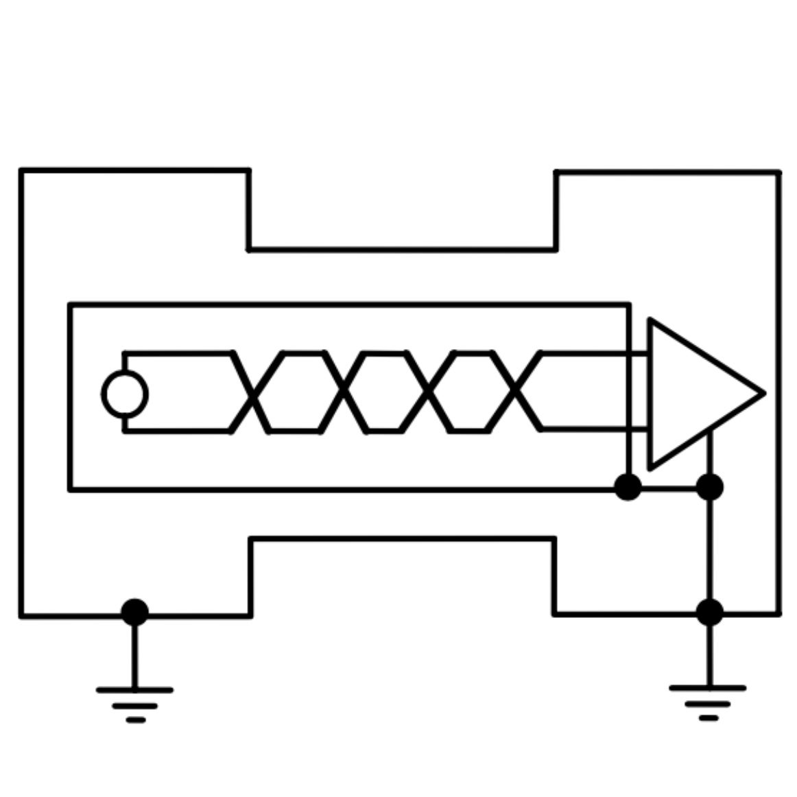
Grounding and Shielding of Electronic Systems
Learn proven techniques for grounding and shielding electronic systems to achieve electromagnetic compatibility.
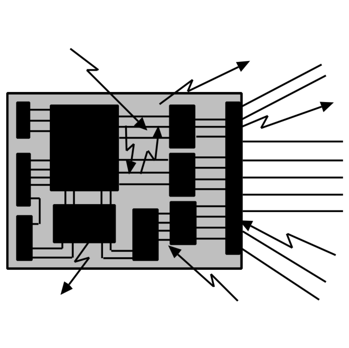
Circuit Board Layout to Reduce EMI
Master PCB layout techniques that minimize electromagnetic interference and ensure EMC compliance.
What You'll Learn
Upon completing both courses, you will be able to:
- Diagnose noise coupling paths and apply reduction techniques
- Design grounding strategies that avoid ground loops
- Implement shielding and filtering best practices
- Optimize PCB layout to reduce EMI/EMC failures
- Build a systematic EMC troubleshooting workflow
Course Outline
20 sessions · 18h of video lectures and demonstrations across both courses
EMC-GS—Grounding and Shielding of Electronic Systems
EMC-PCB—Circuit Board Layout to Reduce EMI
Your Instructor
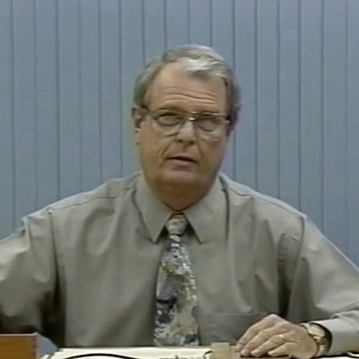
Dr. Tom Van Doren
Professor Emeritus, Missouri S&T
Dr. Tom Van Doren is Professor Emeritus of Electrical and Computer Engineering at Missouri S&T (formerly University of Missouri-Rolla) and a member of the Electromagnetic Compatibility Laboratory. With over 35 years of teaching and industrial experience in electromagnetic compatibility, he brings unparalleled expertise to these courses. He is an inductee of the IEEE EMC Society Hall of Fame.
More than 19,000 engineers and technicians have attended his short courses on grounding, shielding, and PCB layout. His practical approach combines theoretical foundations with real-world demonstrations and examples.
19,000+ engineers trained · IEEE EMC Society Hall of Fame
What Engineers Say
“I think the course is terrific and extremely valuable.”
“It was excellent — you did a tremendous job of explaining things clearly.”
“We hosted Dr. Van Doren 15 years ago. Our new hires need this course.”
Trusted by teams at
 NASA
NASA Boeing
 Ball Aerospace
 Honda
Honda Brookhaven National Lab
 U.S. Air Force
 Matterport
 Plexus
 Schneider Electric
Bundle Pricing
One purchase. 18h of instruction. 1-year access.
Need team or enterprise licensing?
Enterprise Bundle
10+ users — custom pricing
Frequently Asked Questions
How long do I have access?
You have 1-year access from date of purchase. Plenty of time to complete the courses and revisit key topics.
Is this the same content as the in-person course?
Yes — the same lectures and demonstrations, adapted for on-demand viewing at your own pace.
Is the PCB course just a subset of Grounding & Shielding?
No. The G&S course covers PCB layout in two introductory sessions (~2 hours), while the dedicated PCB course is 5 sessions (~5 hours) going much deeper into transmission line effects, DC power distribution, decoupling, component placement, and layer stackup — topics not covered in G&S. They're complementary: G&S is system-level, PCB is board-level.
How much content is in the bundle?
18h of video instruction across 20 sessions, plus downloadable workbooks and certificates for both courses.
Can I expense this?
Absolutely. We can provide an invoice for your employer or procurement team.
Need help deciding? Have questions about team licensing?
Contact Us