PCB EMC Training: Circuit Board Layout to Reduce EMI
by Dr. Tom Van Doren
Starting at $600 / individual · $4,200 / team (up to 10)
Program Overview
This self-paced PCB EMC training course on Circuit Board Layout to Reduce Electromagnetic Emission and Susceptibility helps you base EMC design decisions on logical engineering principles rather than expensive trial-and-error experimentation.
The training spans DC to several GHz frequencies, emphasizing mixed analog/digital designs and multilayer boards. Demonstrations illustrate key concepts, and you'll learn techniques for diagnosing electromagnetic interference at the board level.
Key Skills and Knowledge
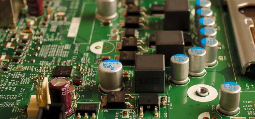
- Reduce EMI issues at the board level
- Optimize signal routing for better EMC
- Design effective power distribution systems
- Select optimal layer stackup configurations
- Apply practical techniques for mixed-signal boards
Learning Objectives
Upon completion, you will be able to:
- Explain why wiring inductance exceeds resistance importance
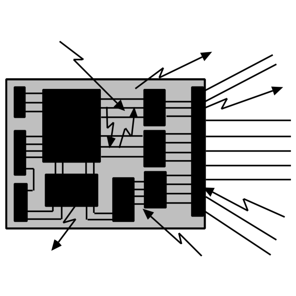
- Describe current loop area's relation to self inductance
- Explain how resonances worsen board emission and immunity
- Determine which nets require transmission line termination
- Describe the four noise-coupling mechanisms
- Explain two ways to reduce each coupling mechanism
- Explain grounding's two purposes
- Differentiate grounding conductors from signal return conductors
- Understand series blocking versus shunt diverting filter techniques
- Recognize trace layouts with excessive inductance
- Design effective DC power-distribution busses
- Understand alternative layer stackup configurations
Course Instructor
Dr. Tom Van Doren
Professor Emeritus, Missouri S&T
Dr. Tom Van Doren is Professor Emeritus of Electrical and Computer Engineering at Missouri S&T (formerly University of Missouri-Rolla) and a member of the Electromagnetic Compatibility Laboratory. With over 35 years of teaching and industrial experience in electromagnetic compatibility, he brings unparalleled expertise to these courses. He is an inductee of the IEEE EMC Society Hall of Fame.
More than 19,000 engineers and technicians have attended his short courses on grounding, shielding, and PCB layout. His practical approach combines theoretical foundations with real-world demonstrations and examples.
What Engineers Say
“I think the course is terrific and extremely valuable.”
“It was excellent — you did a tremendous job of explaining things clearly.”
“We hosted Dr. Van Doren 15 years ago. Our new hires need this course.”
Trusted by teams at
 NASA
NASA Boeing
 Ball Aerospace
 Honda
Honda Brookhaven National Lab
 U.S. Air Force
 Matterport
 Plexus
 Schneider Electric
Course Outline
5 sessions · 5h of video lectures and demonstrations
Who Should Take This Course
This training is ideal for:
- Engineers who design or manufacture electronic equipment
- PCB designers and layout engineers
- Engineers who design metal enclosures for circuit boards
- Engineers who select connectors and cables
- IC and package designers
- Engineers who design filters to reduce conducted emissions
- Engineers who select heat sinks for IC packages
- Engineers who test products for electromagnetic compatibility
Ready to Get Started?
Watch a free lesson to experience the course, or register for full access.
Not sure if this is right for you? Take a quick assessment →